Department of Electronics and Communication
College of Engineering Karunagappally
What You will Learn
- You will understand the theory of binary addition using half adders and full adders.
- You will learn to realize parallel adder on the simulator.
Objectives
Half Adder Circuits
Half adder receives two input bits ($X_n$ and $Y_n$) and produces the sum of the two ($S_n$) and the carry output ($C_n$). It does not add the carry from the previous stage and hence By the inspection of the truth table of half adder in the table below.| $X_n$ | $Y_n$ | $S_n$ | $C_n$ |
| $0$ | $0$ | $0$ | $0$ |
| $0$ | $1$ | $1$ | $0$ |
| $1$ | $0$ | $1$ | $0$ |
| $1$ | $1$ | $0$ | $1$ |
Implementation of Half Adder in QUCS
See the QUCS schematic below. Wire up the circuit using the digital components. ($\fbox{Components}$ $\longrightarrow $ $\fbox{Digital Components}$). Drop the digital switches to simulate the inut signals. Give $Y$ with double the frequency of $X$. Drop $\fbox{Digital Simulation}$ onto the schematic window and run the simulation. Once the simulation is completed, drop $\fbox{tabular}$ on the display window to observe the truth table, as shown below. You may also observe the waveforms.


Full Adder Circuit
The full adder block adds two input bits ($X_{n}$, $Y_{n}$) and the carry output ($C_{n-1}$) from the previous adder block and produces the sum bit $S_{n}$ and the carry output ($C_n$). The truth table is shown below.
| $X_n$ | $Y_n$ | $C_{n-1}$ | $S_n$ | $C_n$ |
| $0$ | $0$ | $0$ | $0$ | $0$ |
| $0$ | $0$ | $1$ | $1$ | $0$ |
| $0$ | $1$ | $0$ | $1$ | $0$ |
| $0$ | $1$ | $1$ | $0$ | $1$ |
| $1$ | $0$ | $0$ | $1$ | $0$ |
| $1$ | $0$ | $1$ | $0$ | $1$ |
| $1$ | $1$ | $0$ | $0$ | $1$ |
| $1$ | $1$ | $1$ | $1$ | $1$ |
The K-map reduction yields the sum bit $S_{n}$ as \begin{align*} S_{n}&=C_{n-1}.(\overline{X_{n}}.\overline{Y_{n}}+X_{n}.Y_{n}) +\overline{C_{n-1}.}(\overline{X_{n}}.Y_{n}+X_{n}.\overline{Y_{n}})\\ &=A_{n}\oplus B_{n} \oplus C_{n-1} \end{align*} The carry bit $C_{n}$ is obtained by reducing the K-map as \begin{align*} C_{n}=X_{n}.Y_{n}+Y_{n}.C_{n-1}+X_{n}.C_{n-1} \end{align*}
Simulation of Full Adder on QUCS
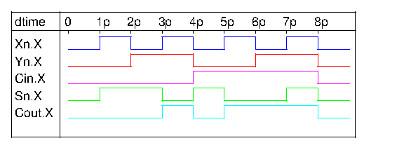
See the QUCs schematic for the full adder given below. Wire up this circuit and perform the digital simulation. Observe the tabular and waveform outputs on the display window.


Now that we understood the operation of the full adder block it is time we use it as a subcircuit to develop multibit parallel adder.
Four Bit Parallel Adder
A multibit adder is realized using a full adder which is realized as a subcircuit. You need to start a project to work with subcircuits. Go to $\fbox{project}$ $\longrightarrow$ $\fbox{new project}$ and give a suitable name to the project and save the project. All relevant files and subcircuits should reside in this project folder or directory.
Generation of Full Adder Subcircuit
Replace the signals from the previous full adder circuit with input and output ports. You delete the signals in the schematic. Go to $\fbox{insert}$ $\longrightarrow $ $\fbox{port}$ to insert a port in the schematic. By default, it is an analog port. Right click on it and change the type as input or output digital port. See the modified schematic below.


Simulation of Four Bit Full Adder
Several digital sources are connected to the input lines to test the four bit adder for different input combinations. Run the digital simulation and drop $\fbox{Tabular}$ in the display window. Select the bit patterns $a_{3}a_{2}a_{1}a_{0}$, $b_{3}b_{2}b_{1}b_{0}$ and $C_{out}S_{3}S_{2}S_{1}S_{0}$. Observe that the latter pattern is the sum of the two four bit patterns. A sample of the tabular output is shown below. Verify the operation.

What You Learned
Comments
Post a Comment